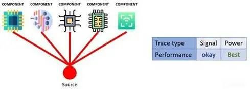
When designing a PCB, we usually rely on previous experience and tips that we would normally find online. Every PCB design can be optimized for a specific appli...
Detail +12-11
1、 Why do circuit boards require a very flat surfaceThe circuit board prototype manufacturer tells you that if the printed circuit board is not flat on the auto...
12-11
1. Engineering design: Precautions for printed circuit board design:A. The arrangement of interlayer semi cured sheets should be symmetrical, for example, for a...
12-09
a) Ma Keng: Ma Keng is the result of organic pollution. A large pit usually indicates oil pollution. If the stirring is poor, the bubbles cannot be expelled, wh...
12-07
Conducting hole (VIA) is a common type of hole used to conduct or connect copper foil circuits between conductive patterns in different layers of a circuit boar...

