Time:2022-01-18Views:
HDI stands for High Density Interconnection, and the technology is rapidly gaining popularity in the printed circuit board world. In general, HDI PCBs can bring a range of benefits to the technology. After all, they help simplify boards so they can do more and take up less space. This means that boards tend to be smaller, which means that the electronics that use these types of boards tend to be smaller. They can perform just fine, but they have smaller, more streamlined packages. Consider how many different types of devices have gotten smaller and smaller over the past decade. One of the reasons is to use HDI PCB.
What is HDI PCB?
High Density Inverter boards can provide a large number of interconnects in a small space. Components are placed closer together on the board, which helps reduce size, but has the same functionality as the larger board. If a circuit board has 120 to 160 pins per square inch, then it's an HDI PCB.
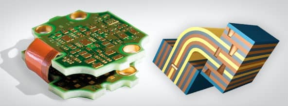
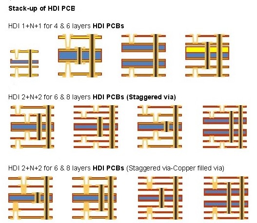
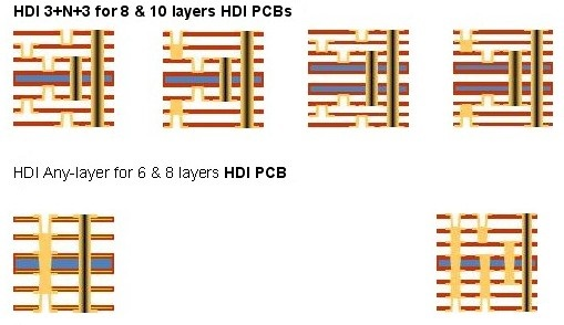
When using universal routing, components are placed together. These types of boards are made possible with the help of microvia technology to blind buried vias. They are very efficient and are becoming more popular in a variety of different industries, as shown below.

HDI board process


The biggest advantage of HDI PCBs
Many people want to find ways to reduce the manufacturing area of their products, and one of the best ways is to use HDI PCBs. They are a great solution when you need to reduce size and weight, and still need the functionality and reliability of the product. One of the other advantages of these boards is that they use solder-in-pad technology and blind via technology. This allows components to be placed together, thereby reducing the length of signal paths, which helps provide faster and more reliable signals because those paths are shorter.
Even though these boards can offer a lot of advantages, you will still find that they are still very affordable. It's a cost-effective solution for those looking for a reliable and durable option for their electronics. Still, to decide if they're right for you, it's important to learn more about them and how to use them. You also need to understand the difference between regular printed circuit boards and HDI printed circuit boards.
Where are HDI PCBs used today?
Because of the benefits they provide, you will find HDI PCBs utilized in a variety of electronic devices in many different industries. The medical industry is one of the most well-known industries. Medical devices manufactured today often require smaller circuit boards. Whether it's a piece of equipment in the lab or an implant, the smaller size is often the better option, and HDI PCBs can be of great help here. Pacemakers are a good example of the type of products that use these types of PCBs. This technique is used by many types of monitoring and exploration equipment, such as endoscopes or colonoscopes. Again, in these cases, smaller is the better choice.
In addition to the healthcare sector, the automotive industry also uses HDI PCBs. To maximize the available space in the car, they are making certain electronic components smaller. Of course, tablets and smartphones use this technology. That's why many of these devices are getting thinner and thinner as they go.
You will also find HDI PCBs for aerospace and military applications. Their reliability and small size allow them to be used in many different applications. In the future, more and more devices from different fields may use this technology.
What's more, HDI is also applied in military. Having a solid and compact structure doesn’t allow an HDI PCB to break down or get damaged easily. Therefore, it comes to use in military sectors where dangers and damages are nothing unexpected. Additionally, it gets used in missile launching, defense networks, and other communicating purposes.
The difference between HDI and standard PCBs
To better understand some of the key differences between these two options, consider the list below.
HDI PCBs have denser components per square inch
These boards end up being smaller and lighter than typical PCBs
They utilize laser direct drilling, whereas standard PCBs are usually mechanically drilled
Both the number of layers and the aspect ratio tend to decrease
These are some of the differences between HDI PCB and regular PCB. However, that doesn't mean the HDI option is always the right choice for you. Take the time to think about the project you're working on, and then decide which option best suits your needs.
Designing using HDI
HDI contains a myriad of formation that influences the entire density of the PCB. Therefore, while designing an HDI, one must keep some points in mind. These are:
l Remember that space is the fundamental prerogative.
l You must understand the indication of the buried and blind vias.
l You must avoid any kind of solder-related issues.
l Review your plan.
Once you follow these processes, nothing can stop you from creating a perfect HDI printed circuit board.
Hopefully, the whole concept about HDI, its benefits, design tips, applications, and how it stands apart from standard PCBs are evident so far. However, don’t expect to understand everything in detail unless you are an engineer and HDI manufacturer. If you are in search of making a faultless HDI, make sure to look for help. Always contact a professional for the best result.
Optimization and improvement of HDI technology in our HDI flex-rigid PCB boards
1. 1+4+1 buried hole HDI two core board structures are optimized into one core board structure.
2. It is forbidden to use the middle hole process of the outer through-hole plate for the inner buried hole (H60294 uses this process to cause the client to explode), and it is forbidden to use the buried hole of the solder mask. Process cards have been updated.

