Time:2021-12-17Views:
For designers, to successfully design a flexible PCB, a basic understanding of flexible design requirements is required. This article will explain some of these basic design guidelines.
Flexible PCBs were originally used in the military industry, but today they are used in almost every industry. With that in mind, let's take a closer look at these 10 design requirements:
1. Prerequisites for Resilient Design
2. The dimension drawing must define a rigid-to-flexible interface
3. Flexible PCB stack-up structure and layer sequence
4. Explanatory Notes from flexible PCB Manufacturers
5. Flexibility and Bending Radius
6. Dimensional stability
7. Need to be shielded
8. Drilling symbol diagram
Considerations for Flexible Design
1. Prerequisites for Resilient Design
First, there are several board elements that must be included in the design. These include:
a. Layer
b. Thickness of finished board
c. PCB material usage
d. Surface finish
e. Drill size
f. drill copper
These may seem like obvious requirements, but are sometimes ignored. When this happens, the PCB manufacturer will need to follow up for clarification, delaying turnaround times.
2. The dimension drawing must define a rigid-to-flexible interface
Dimensional drawings identify many key measurements of a PCB design. The dimension drawing should define a rigid to flexible interface. It should describe where these two types of material meet. Typical profile tolerances are +/- 0.010 inches.
Dimensional drawings for flexible PCB designs provide the following information:
a. Location and size of stiffeners
b. Thickness of each part of the PCB and materials used

c. Type of static or dynamic flexibility during circuit operation. A PCB that is bent up to 20 times is called a semi-static flex PCB. A PCB that bends and twists regularly is called a dynamic bend PCB. The printer uses dynamic flex PCBs because the circuit bends throughout the operation of the printer.
d. A location where the circuit board is seldom and often bent.
3. Flexible PCB stack-up structure and layer sequence
Stacking distinguishes between rigid and flexible layers in a PCB. A flexible PCB stackup diagram will give the thickness of each layer, including the copper weight of the conductive layers. It will also indicate the impedance curve and impedance value (50 ohms or 100 ohms).
4. Explanatory Notes from flexible PCB Manufacturers
PCB manufacturers want descriptive notes on:
a. Class type (class 1, class 2, class 3), wiring type and installation and use requirements
b. Flexible copper clad material used
c. Cover material
d. Maximum plate thickness
e. Minimum size of plated through hole
f. Electrical test requirements
g. Cover color
h. Silk printing color
i. Board markings such as part number, version and company logo
j. Packaging and shipping needs
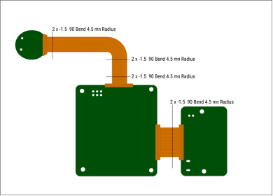
5. Flexibility and Bending Radius
The flexibility of a flexible PCB depends on the bend radius of the flexible material used. The bend radius is the smallest angle the bendable area can bend.
Knowing how many times a flex PCB is bent is critical to your design. If the PCB is bent more times than the design allows, the copper will start to stretch and crack.
The bend radius depends on the number of layers and the type of material used in the flexibility.

6. Dimensional stability
Dimensional stability is an extremely important factor that designers must address, especially in high-density designs. Small dimensional changes can easily occur in circuit boards during processing. Additionally, these PCBs are exposed to various processes, including etching, plating, pressure, temperature, and chemistry. It becomes important for designers to consider the above changes to determine part numbers for new flex circuits.
Implement scale factor
Designers must apply various scaling factors on the second layer of the PCB board. These dimensional changes occur in the PCB when it is cured during the thermal lamination process. Designers and manufacturers must employ several in-process measurements with the help of scale factors. These scaling factors help manufacturers predict loss percentages and scale up PCB sizes based on designer requirements. These calculations are performed through dynamic methods. Performing the final drilling procedure in the multilayer circuit also helps to improve dimensional stability.
Software assistance
Perform various software-controlled operations and calculations to analyze dimensional shifts. These calculations are performed with the help of optical fiducials. These methods involve measuring targets present on the outside corners of the panel. After a few plots, the alignment is correct, allowing the necessary X, Y and theta corrections.
7. Need to be shielded
Shielding is another important parameter to consider for flex circuits. Implement various methods to incorporate masking. Shields are used to limit the effects of EMI and ESD. The shield also helps keep the controlled impedance requirement constant.
Designers typically perform four types of shielding, including:
a.Copper cladding
b. Copper hatch
c. Silver paste/epoxy resin
d. EMI thermoplastic shielding film
8. Drilling symbol diagram
The drilling symbol table indicates all finished hole sizes and hole size tolerances for the board design. To learn more about PCB drilling, read PCB Drilling Instructions: Do's and Don'ts. The Drilling Symbols table summarizes the drilling information that exists on the board.
Considerations for Flexible Design
a. Avoid placing vias in curved areas of flex circuits. However, if you need to place vias in a flex circuit, make sure there is no bend in the area to place the vias.
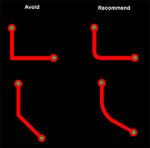
b. Always use curved traces rather than traces with corners.

c. Avoid sudden changes in trace width.
d. The minimum clearance between the copper ring and the nearest via should be 20 mils.
Conclusion
When we design flex PCBs, it is crucial for us to provide manufacturers with important information (drawing requirements) as this information helps them to manufacture flex PCBs as the designer expects without any time Delay.

