

Time:2023-07-25Views:
In 1941, the United States painted copper paste on talcum as wiring to make proximity tubes.
In 1943, Americans extensively used this technology in military radios.
In 1947, epoxy resin began to be used as a substrate for manufacturing. At the same time, NBS began researching manufacturing techniques such as forming coils, capacitors, and resistors using printed circuit technology.
In 1948, the United States officially recognized this invention for commercial use.
Since the 1950s, transistors with lower heat generation have largely replaced vacuum tubes, and printed circuit board technology has only begun to be widely adopted. At that time, etching foil film technology was the mainstream.
In 1950, Japan used silver paint as wiring on glass substrates; Copper foil is used as wiring on paper phenolic substrates (CCL) made of phenolic resin.
In 1951, the appearance of polyimide further improved the heat resistance of the resin, and also produced polyimide substrate.
In 1953, Motorola developed a double-sided board with electroplated through hole method. This method is also applied to later multi-layer circuit boards.
In the 1960s, after 10 years of widespread use of printed circuit boards, their technology became increasingly mature. Since the introduction of Motorola's double-sided boards, multi-layer printed circuit boards have emerged, increasing the ratio of wiring to substrate area.
In 1960, V Dahlgreen creates a soft printed circuit board by sticking a metal foil film with printed circuits onto thermoplastic plastic.
In 1961, Hazeltine Corporation in the United States referred to the electroplating through hole method to produce multi-layer boards.
In 1967, one of the layering methods, "Plated up technology," was published.
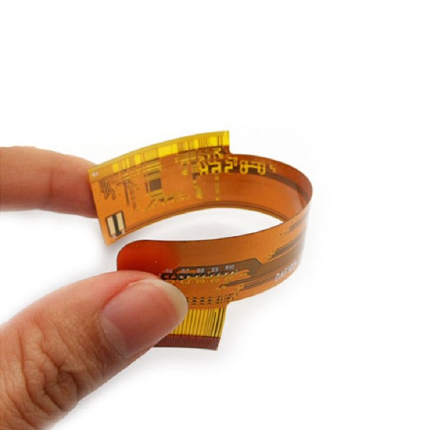
In 1969, FD-R manufactured flexible printed circuit boards with polyimide.
In 1979, Pactel published one of the layering methods, the "Pactel method".
In 1984, NTT developed the "Copper Polymide method" for thin film circuits.
In 1988, Siemens developed the layering PCB of Microwiring Substrate.
In 1990, IBM developed an additional layer printed circuit board for Surface Laminar Circuit (SLC).
In 1995, Panasonic developed the layer added printed circuit board of ALIVH.
In 1996, Toshiba developed an additional layer printed circuit board for B2it.

E-EMAIL: xcfeirc-fpc@vip.163.com
Jampzhang@xcfefpc.com
TEL: +86-13560713321


Product

Process Capability
About Us
News
Contact Us
 中
中